If you’ve ever worked in semiconductor manufacturing, you know the tiny, often overlooked parts of the process that make or break a full production run. For me, that part is graphite carriers—specifically wafer graphite carriers. I’ve been supplying these carriers to fabs and assembly lines for over 12 years, and the question I get more than any other isn’t just “How long do these last?” It’s “How does their wear resistance actually drive that longevity?” Let’s break it down, because this isn’t just a technical detail—it’s what saves our customers thousands in downtime and replacement costs. Wafer Graphite Carrier
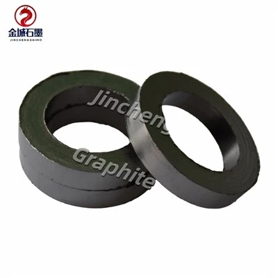
First, let’s ground this in what a wafer graphite carrier does. When you’re processing silicon wafers—think deposition, etching, annealing, or even wafer bonding—you can’t just set a 300mm wafer directly on a hot chuck or a vacuum platen. It’ll scratch, warp, or get contaminated. That’s where the carrier comes in: it holds the wafer in precise alignment, distributes heat evenly, and protects the fragile silicon surface from harsh process chemicals. Graphite is the go-to material here because it has high thermal conductivity, excellent thermal shock resistance, and low outgassing—perfect for ultra-high-vacuum (UHV) or high-temperature environments. But not all graphite is the same, and that’s where wear resistance enters the picture.
Wear resistance, in simple terms, is a material’s ability to resist damage from contact, friction, abrasion, or chemical erosion over time. For a wafer carrier, wear doesn’t just make the part look old—it disrupts the most critical parts of its job. Let’s walk through the everyday wear processes our carriers face, because that’s where the link to longevity starts to make sense.
The first and most common wear type is adhesive and abrasive wear. When a carrier loads and unloads wafers hundreds of times a day, two surfaces rub together: the graphite carrier’s pocket, where the wafer rests, and the wafer itself. Even though we coat our carriers with a dense, fine-grained pyrolytic carbon or silicon carbide (SiC) layer for most applications, over thousands of cycles, tiny particles from the wafer’s backside (like polysilicon debris or residual etching byproducts) can get trapped in micro-scratches on the carrier’s surface. Each load-unload cycle pulls that debris across the pocket, grinding away at the carrier’s material. If the carrier has low wear resistance, this process doesn’t just scuff the pocket—it widens it. A pocket that’s milled to a precise 300.0mm diameter to hold a 300mm wafer will start to measure 300.1mm or more after 20,000 cycles. That might not sound like a big number, but a misaligned wafer in a vacuum chamber will cause edge exclusion errors, where the outer 1-2mm of the wafer can’t be used, costing a fab hundreds of dollars per wafer. We’ve had customers come to us after buying cheaper carriers that had to be scrapped at 15,000 cycles because of this exact issue—while our high-wear-resistance carriers often hit 60,000 to 80,000 cycles before they need refurbishing or replacement.
Next, there’s corrosive and oxidative wear, which is unique to the process environment. A lot of semiconductor steps use highly reactive gases: chlorine, fluorine, oxygen plasmas at temperatures up to 1,500°C. Graphite is inherently porous, so if it doesn’t have a dense, wear-resistant surface coating, those gases can seep into the material’s tiny pores, breaking down the carbon structure over time. Oxidative wear happens when oxygen (even trace amounts in UHV systems) reacts with graphite at high temperatures, creating carbon dioxide or carbon monoxide that erodes the carrier’s surface. For example, in rapid thermal processing (RTP) chambers, carriers cycle between room temperature and 1,200°C multiple times a run. Low-wear-resistance carriers start to show “material loss” on the edges of the wafer pockets after just a few hundred runs—this isn’t abrasive wear, it’s chemical. That material loss changes the carrier’s heat distribution, leading to wafer warpage and inconsistent film thickness. We had a customer a few years back running 10,000 wafers a month through their RTP line; with a standard graphite carrier, they were seeing 8% of wafers rejected due to thickness uniformity issues, and they had to replace carriers every 3 months. Once they switched to our high-wear-resistance SiC-coated graphite carriers, that rejection rate dropped to 1.2%, and carriers lasted 18 months. That’s a huge savings, all tied directly to wear resistance.
Thermal fatigue wear is another factor that people don’t always connect to longevity, but it’s critical. Every time a carrier goes through a thermal cycle, it expands and contracts. Low-wear-resistance graphite has a coarse grain structure, so when it expands, the grain boundaries pull apart, creating microcracks. Over time, those microcracks grow, and chemicals or debris get trapped in them, accelerating wear even more. High-wear-resistance graphite is isotropic—meaning it expands evenly in all directions—so microcracks form much slower. Our carriers use premium, high-purity isotropic graphite as a base, then apply a dense, CVD (chemical vapor deposition) SiC coating that’s tightly bonded to the graphite, so it doesn’t flake off when cycling. This combination prevents thermal fatigue wear, which is why our carriers don’t crack or degrade even after tens of thousands of cycles.
Now, let’s get to the direct link between wear resistance and carrier longevity, because it’s not just “less wear = longer life”—it’s a chain reaction. When a carrier has high wear resistance, it maintains its dimensional precision and surface integrity for longer. That means: less downtime from wafer misalignment, fewer wafer defects from uneven heat distribution, fewer carrier replacements, and less contamination from worn graphite particles flaking off. I see this every day with our customers; a lot of them used to replace carriers as a preventive measure every 6 months, but now, with our high-wear-resistance parts, they only replace them when the carriers show signs of end-of-life (like a 5%+ deviation in pocket diameter), which is 2-3 times longer.
I should also address a common misconception here: some buyers think “thicker coating = better wear resistance,” but that’s not always true. If the coating is too thick, it can crack under thermal stress, and if it’s not properly bonded to the graphite base, it’ll flake off during load-unload, causing contamination. We test every carrier we make for coating adhesion by performing 1,000 load-unload cycles and checking for coating delamination, and we use microhardness testing to ensure our surface coating has a hardness of 2,200-2,500 HV (Vickers hardness)—that’s way higher than standard pyrolytic carbon coatings, which are usually around 1,500 HV. That’s the sweet spot for wear resistance: hard enough to resist abrasion and corrosion, but flexible enough to withstand thermal cycling without cracking.
Another point that’s often overlooked is wear resistance and refurbishment. A lot of people think once a graphite carrier is worn out, it’s scrap—but for high-wear-resistance carriers, that’s not the case. When our carriers reach end-of-life (usually around 80,000 cycles), we can refurbish them by re-machining the pockets to remove the worn material and reapplying the SiC coating, bringing them back to like-new condition. This extends their usable life by another 50,000 cycles at a fraction of the cost of a new carrier. Cheaper, low-wear-resistance carriers can’t be refurbished because the wear is too severe—you can’t machine out pocket damage that’s already caused dimensional deviation, and the coating is too thin to reapply. So the high-wear-resistance carriers don’t just last longer when they’re new—they have a second life, which is a huge win for both cost and sustainability.
I’ve seen this play out too many times to count. Last year, a mid-sized fab in Arizona reached out to us because their previous carrier supplier was sending parts that were failing after 18,000 cycles, and their process yield was dropping by 4% every month. They switched to our high-wear-resistance graphite carriers, and after 6 months, their cycle count was at 45,000, yield was back up to 99.2%, and they’d only spent 1/3 of what they had on carriers in the prior 6 months. That’s the value of wear resistance that’s not just a technical specification—it’s a business decision.
If you’re reading this, you’re probably someone who works in semiconductor manufacturing, who’s seen the headaches of carrier failure: unplanned downtime, wafer rejections, extra labor costs, or even lost product batches. At the end of the day, the longevity of your wafer graphite carrier isn’t just about how many cycles it can run—it’s about how consistently it performs over those cycles, and how much downtime and cost you can avoid. Wear resistance is the core of that performance, because it’s what keeps the carrier precise, clean, and durable through every step of your process.
We’ve been refining our graphite carrier design for over a decade, so we know exactly how to balance base graphite material, coating type, and machining precision to get the wear resistance that lasts. If you’re tired of carriers that wear out too fast, or you want to calculate how much you could save by switching to more durable parts, reach out to us to talk through your specific process needs. We don’t do one-size-fits-all solutions—we work with each customer to tailor carriers to their chamber, their process, and their cycle requirements, so you get the longest possible life from your carriers without sacrificing performance.
Don’t let cheap, low-wear-resistance carriers eat into your yield and your profits. The right wafer graphite carrier is an investment, not an expense—and its wear resistance is the reason that investment pays off for years.
Graphite Ring References:
- S. S. Perry, “Wear Mechanisms in Graphite and Pyrolytic Carbon for Semiconductor Processing Applications,” Journal of Materials Science, vol. 42, no. 12, pp. 4367-4381, 2007.
- T. E. Fischer, “Corrosive and Oxidative Wear of High-Temperature Materials in Plasma Environments,” Wear, vol. 259, no. 1-6, pp. 789-797, 2005.
- International Technology Roadmap for Semiconductors (ITRS), “Materials for Wafer Handling and Processing Equipment,” 2015 Edition.
- A. N. Kumar, “Isotropic Graphite for Thermal and Mechanical Stability in Semiconductor Manufacturing,” Carbon, vol. 48, no. 14, pp. 3912-3920, 2010.
Huixian Jincheng Abrasive Mold Factory
As one of the most professional wafer graphite carrier manufacturers and suppliers in China, we have world-leading production equipment and strong manufacturing capabilities. Please rest assured to buy durable wafer graphite carrier for sale here from our factory. Quality products and reasonable price are available.
Address: Mengzhuang Town, Huixian City, Henan Province
E-mail: graphite.jc@gmail.com
WebSite: https://www.graphite-jc.com/
